The AMD Ryzen 9 9850HX is a high-end notebook processor from the Fire Range series with 12 of 16 cores and hyperthreading (SMT), which means it can process up to 24 threads simultaneously. Unlike the Ryzen 9 9955HX3D, the chip does not offer a 3D V-Cache. The chip was presented at CES in early 2025 and is intended for fast and expensive gaming laptops.
The CPU uses the new Zen 5 architecture for the 12 cores and clocks them at up to 5.2 GHz (single-core boost).
Thanks to the 12 fast Zen 5 cores, the performance should be excellent and well suited for all demanding applications. We assume that the performance will be similar to the old Ryzen 9 7845HX (12 x Zen 4 with up to 5.2 GHz) is similar. The faster Ryzen 9 9955HX and 9955HX3D should be able to set themselves apart significantly due to the higher number of cores (with multi-thread performance).
The 9850HX is intended for large and heavy gaming notebooks and is therefore configurable from 45 - 75 watts TDP (default 55 watts). The SoC is manufactured in the modern 4nm FinFET process at TSMC (both compute dies, I/O die in 6nm) and should therefore have very good energy efficiency.
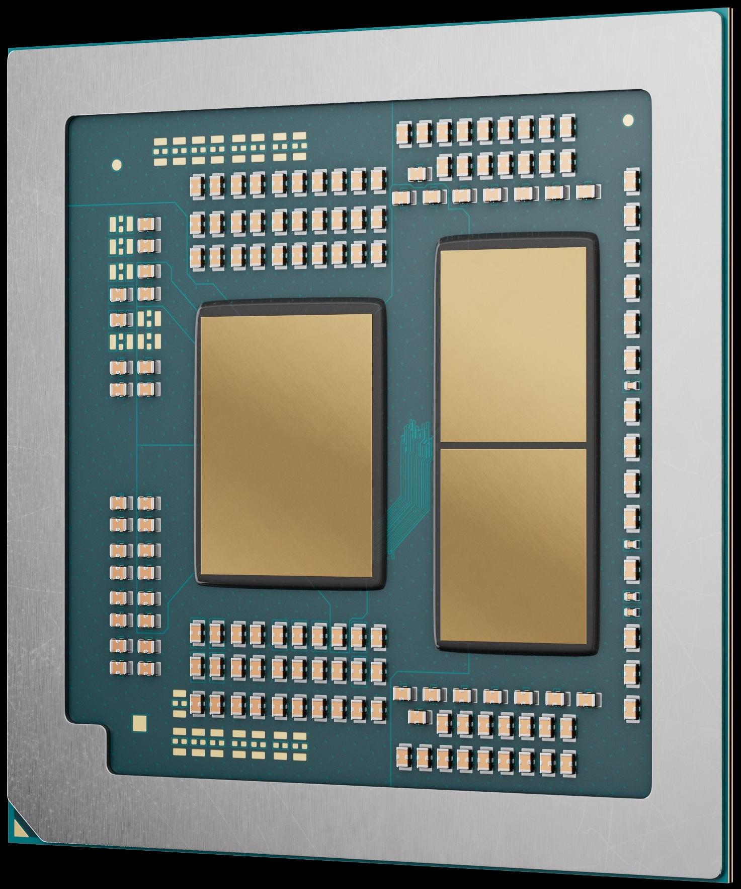
The AMD Ryzen 9 9955HX3D is a high-end notebook processor of the Fire Range series with 16 cores and hyperthreading (SMT), which means it can process up to 32 threads simultaneously. The CPU uses the new Zen 5 architecture for all 16 cores and clocks them at 2.5 to 5.4 GHz (single-core boost). As a special feature, the HX3D has an additional 64M 3D V-Cache on a CCD. This means that the CPU offers combined 128 MB L3 cache and 16 MB L2 cache. The chip was presented at CES in early 2025 and is intended for fast and expensive gaming notebooks.
AMD claims that the Ryzen 9 9955HX3D is the fastest mobile gaming CPU. Based on the experience with its predecessor, the Ryzen 9 7945HX3D, this is quite realistic. The 3D V-Cache in particular can accelerate demanding 3D games. However, the 16 fast Zen 5 cores should also provide enough power for all possible demanding applications.
The 9955HX3D is intended for large and heavy gaming notebooks and can therefore draw quite an amount of power (configurable from 55- to 75 watts TDP, default 55 watts). The SoC consists out of three dies on a package where the processor dies are manufactured in the modern 4nm 4nm FinFET process at TSMC (I/O die in 6nm) and should therefore still have a good energy efficiency.
- Range of benchmark values for this graphics card - Average benchmark values for this graphics card * Smaller numbers mean a higher performance 1 This benchmark is not used for the average calculation
v1.34
log 19. 12:52:29
#0 ran 0s before starting gpusingle class +0s ... 0s
#1 checking url part for id 18733 +0s ... 0s
#2 checking url part for id 18729 +0s ... 0s
#3 not redirecting to Ajax server +0s ... 0s
#4 did not recreate cache, as it is less than 5 days old! Created at Sun, 19 Oct 2025 05:20:51 +0200 +0s ... 0s
#5 composed specs +0.004s ... 0.004s
#6 did output specs +0s ... 0.004s
#7 getting avg benchmarks for device 18733 +0.001s ... 0.004s
#8 got single benchmarks 18733 +0.003s ... 0.007s
#9 getting avg benchmarks for device 18729 +0.003s ... 0.011s
#10 got single benchmarks 18729 +0.006s ... 0.017s
#11 got avg benchmarks for devices +0s ... 0.017s
#12 min, max, avg, median took s +0.024s ... 0.041s